


INDUSTRIES SERVED
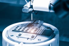
Microelectronics
Expert failure analysis for today's most complex devices.
Microelectronic product failures hurt more than your bottom line; they can destroy your reputation and lead to costly litigation.
Devices use nanomaterials with multiple metal layers deposited over hundreds of sequenced processing steps. Complex, multilayer manufacturing makes root‑cause microelectronic failure analysis challenging. RJ Lee Group’s experts go beyond providing analytical data; we help you to uncover the root causes of failure in today's most complex microelectronic devices:
- Raw materials testing and analysis
- Process‑induced defect analysis
- QA/QC support and augmentation
- Evaluation of finished and returned products
- Turning complex, multilayer manufacturing challenges into clear failure insights.
RJ Lee Group delivers expert insight to resolve complex microelectronic failures.

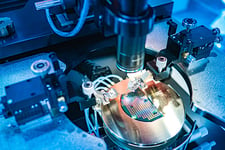
Root Cause Analysis, Layer by Layer
Materials Analysis
Improve product performance through detailed analysis of wafer substrates, residual contaminant films, point defects, and crystallographic features such as orientation and inherent stress.
Thin Film Layers and Structures
Understand the compositional and physical characteristics of deposited or grown thin film layers to isolate and identify areas of concern or improvement.

Solder Materials
Identify defects in solder connections and evaluate lead content quality to improve them.
Metallization Contacts, Traces, and Interconnects
Locate defects and failures and evaluate whether their source is process or service related.
IC Packages
Characterize chip failures through destructive physical analysis.
Packaging and Products
Eliminate odors and precipitated film residues by conducting destructive physical analysis.
Raw Materials
Ensure ROHS compliance by determining the precise concentrations of restricted substances.
Client Success Stories

Resolving Failures in Today's Most Complex Devices
Microelectronic failures don't follow simple patterns. A defect might originate in the substrate, a deposited layer, a metallization step, or a packaging process, and pinpointing which one requires the right combination of instrumentation and materials expertise. Our services include:
Semiconductor Failure Analysis

Systematic investigation of device failures using advanced microscopy and spectroscopy to identify root causes at the nanoscale.
Material and Component Characterization
Composition, structure, and defect analysis across wafer substrates, thin films, solder, metallization, and packaging.
Contamination Analysis and Control
Identifying and tracing contaminant sources that impact yield, reliability, or device performance.
Reliability Testing and Quality Assurance
QA/QC support and testing to verify that devices meet performance and durability specifications.
Process Optimization
Analysis of process-induced defects and manufacturing variables to improve yield and reduce failure rates.
Technologies
Scanning Electron Microscopy (SEM/EDS)

Electron Backscatter Diffraction (EBSD)
X-Ray Diffraction (XRD)
ICP-Mass Spectrometry (ICP-MS)
Discuss Materials Analysis & Testing with an Expert
