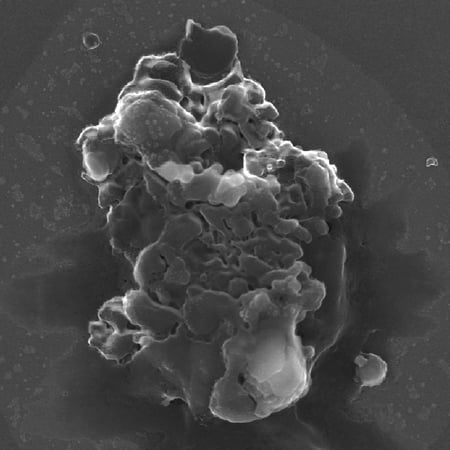
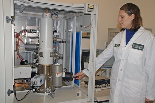
Scanning Electron Microscopy (SEM) is a powerful imaging technique that enables the examination of surfaces and materials at extremely high magnification. SEM uses a focused beam of electrons to create detailed images, revealing features and structures that are invisible to the naked eye. This technology enables the identification of contamination, analysis of failure points, and investigation of material composition with remarkable clarity. At RJ Lee Group, SEM is crucial for supporting quality control, troubleshooting, and research across various industries, including manufacturing, pharmaceuticals, electronics, and construction.
Instrumentation
Scanning Electron Microscopy (SEM)

What is SEM?
A scanning electron microscope (SEM) operates by directing a focused beam of high-energy electrons onto the surface of a sample and detecting the various signals emitted as the electrons interact with the material. These interactions produce secondary electrons, backscattered electrons, and characteristic X-rays, each offering different insights into the sample’s topography and composition.
The SEM image reveals surface features at nanometer-scale resolution, allowing for precise analysis of morphology, texture, and elemental distribution. SEM is widely used in materials science, biology, and forensic investigations due to its ability to deliver both qualitative and quantitative data with exceptional clarity.
What is CCSEM?
Computer-Controlled Scanning Electron Microscopy (CCSEM) combines the resolution of the SEM with the efficiency of computer automation. IntelliSEM™ software, developed by RJ Lee Group, automates the process of scanning a sample and identifying particles, categorizing shapes, finding inclusions, or other preset criteria for later analysis.
What Can You Do With SEM?
Scanning electron microscopy (SEM) is widely used for high-resolution imaging and surface characterization across many industries:
- Materials Science: Analyze microstructures, grain boundaries, and fracture surfaces to understand mechanical properties and failure mechanisms.
- Pharmaceuticals: Examine particle size, morphology, and coating uniformity in drug formulations to ensure consistency and quality.
- Polymers and Plastics: Investigate filler dispersion, surface defects, and degradation patterns to optimize performance and troubleshoot failures.
- Environmental Testing: Characterize airborne particulates, microplastics, and mineral content in soil or sediment samples.
- Electronics and Semiconductors: Inspect circuit features, solder joints, and contamination at the microscale to support quality control and reliability.
- Forensics: Identify trace evidence such as gunshot residue, fibers, or tool marks to support criminal investigations.


Why Choose RJ Lee Group for SEM Analysis?
At RJ Lee Group, we don’t just perform Scanning Electron Microscopy (SEM), we redefine its potential. With over 35 years of experience in materials characterization and scientific consulting, our team brings unmatched expertise, innovation, and precision to every SEM analysis
- Pioneers in SEM Innovation
RJ Lee Group commercialized the first computer-automated SEM. This legacy of innovation continues today with our proprietary IntelliSEM® software. - Advanced Capabilities for Complex Challenges
Our SEM services are designed to deliver actionable insights. We combine SEM with complementary techniques like EDS, XRD, FTIR, and thermal analysis to provide a full-spectrum understanding of your materials. - Trusted by Industry Leaders
Our work has supported Fortune 500 OEMs in extending jet engine life, helped uncover the root causes of infrastructure failures, and contributed to cutting-edge research aboard the International Space Station. - Data-Driven, Decision-Ready
Our SEM analyses are backed by SEAMS, a proprietary big data platform that integrates structured and unstructured data to support real-time decision-making in next-generation manufacturing.
The Dr. Richard J Lee
Microscopy Center of Excellence
Established in 2021, the Richard J Lee Microscopy Center brings together the bulk of our SEM instruments into a single location, giving our experts easy access to a variety of capabilities and fostering collaboration. Combined with SEM capabilities in our powdered materials lab, CBAL lab, and mobile labs, RJ Lee Group boasts one of the largest collections of scanning electron microscopes in the United States.
Get in Touch
Since our inception, RJ Lee Group has set the industry standard in scanning electron microscopy (SEM), evolving from a single-instrument lab to a nationwide network equipped with advanced SEM technologies. For more than four decades, we have driven innovation in SEM applications across diverse industries. Connect with our team to discover how our specialized expertise, automated solutions, and comprehensive technical capabilities provide actionable insights and results unmatched by other laboratories.

Blog
Read More
10 min read
Unlocking the Secrets of Materials: The Power of X-ray Diffraction (XRD) and X-ray Fluorescence (XRF)
October 01, 2024


